93
9152BINDCO02/10
ATA8743
generation. Similarly, do not write the TCNT0 value equal to BOTTOM when the counter is
down-counting.
The setup of the OC0x should be performed before setting the Data Direction Register for the
port pin to output. The easiest way of setting the OC0x value is to use the Force Output Com-
pare (0x) strobe bits in Normal mode. The OC0x Registers keep their values even when
changing between Waveform Generation modes.
Be aware that the COM0x1:0 bits are not double buffered together with the compare value.
Changing the COM0x1:0 bits will take effect immediately.
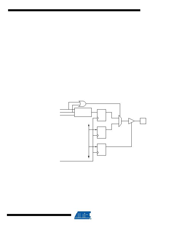
20.6 Compare Match Output Unit
The Compare Output mode (COM0x1:0) bits have two functions. The Waveform Generator uses
the COM0x1:0 bits for defining the Output Compare (OC0x) state at the next Compare Match.
Also, the COM0x1:0 bits control the OC0x pin output source. Figure 20-4 on page 93 shows a
simplified schematic of the logic affected by the COM0x1:0 bit setting. The I/O Registers, I/O
bits, and I/O pins in the figure are shown in bold. Only the parts of the general I/O Port Control
Registers (DDR and PORT) that are affected by the COM0x1:0 bits are shown. When referring
to the OC0x state, the reference is for the internal OC0x Register, not the OC0x pin. If a system
reset occur, the OC0x Register is reset to
0
.
Figure 20-4. Compare Match Output Unit, Schematic
The general I/O port function is overridden by the Output Compare (OC0x) from the Waveform
Generator if either of the COM0x1:0 bits are set. However, the OC0x pin direction (input or out-
put) is still controlled by the Data Direction Register (DDR) for the port pin. The Data Direction
Register bit for the OC0x pin (DDR_OC0x) must be set as output before the OC0x value is visi-
ble on the pin. The port override function is independent of the Waveform Generation mode.
The design of the Output Compare pin logic allows initialization of the OC0x state before the out-
put is enabled. Note that some COM0x1:0 bit settings are reserved for certain modes of
operation, see
Register Description
on page 100
PORT
DDR
D Q
D Q
OCn
Pin
OCnx
D Q
Waveform
Generator
OMnx1
OMnx0
0
1
OCn
lk
发布紧急采购,3分钟左右您将得到回复。
相关PDF资料
ATAVRRZ200
KIT DEMO AT86RF230
AV101-12LF
ATTENUATOR HIP3 0.70-1GHZ 8-SOIC
AV102-12LF
ATTENUATOR HIP3 1.7-2GHZ 8SOIC
AV113-12LF
ATTENUATOR HIP3 2.1-2.3GHZ 8SOIC
AXUV100G
SENSOR ELECTRON DETECTION
B0205F50200AHF
XFRMR BALUN RF 200-500MHZ 1608
B0310J50100AHF
XFRMR BALUN RF 300-1000MHZ 0805
B0322J5050AHF
XFRMR BALUN RF 300-2200MHZ 0805
相关代理商/技术参数
ATAB5275
功能描述:射频开发工具 LF Tx Antenna driver board (TPMS) RoHS:否 制造商:Taiyo Yuden 产品:Wireless Modules 类型:Wireless Audio 工具用于评估:WYSAAVDX7 频率: 工作电源电压:3.4 V to 5.5 V
ATAB5276
功能描述:射频开发工具 1A Antenna Driver Demoboard RoHS:否 制造商:Taiyo Yuden 产品:Wireless Modules 类型:Wireless Audio 工具用于评估:WYSAAVDX7 频率: 工作电源电压:3.4 V to 5.5 V
ATAB5278
功能描述:射频开发工具 LF Tx Antenna driver board (PEG) RoHS:否 制造商:Taiyo Yuden 产品:Wireless Modules 类型:Wireless Audio 工具用于评估:WYSAAVDX7 频率: 工作电源电压:3.4 V to 5.5 V
ATAB5279
功能描述:射频开发工具 LF Transmitter with ATA5279 RoHS:否 制造商:Taiyo Yuden 产品:Wireless Modules 类型:Wireless Audio 工具用于评估:WYSAAVDX7 频率: 工作电源电压:3.4 V to 5.5 V
ATAB5282
功能描述:BOARD EVAL LF 125KHZ ANT DVR 3CH RoHS:是 类别:RF/IF 和 RFID >> RFID 评估和开发套件及电路板 系列:Smart RF 产品培训模块:M24LR64 Dual Interface EEPROM 标准包装:1 系列:- 类型:读取器模块 频率:13.56MHz 适用于相关产品:M24LR-64-R 已供物品:2 根基准天线,I2C 和 RFID 读取器,样品 其它名称:497-10480
ATAB5283
功能描述:射频开发工具 LF Rx Board 1 channel (TPMS)
RoHS:否 制造商:Taiyo Yuden 产品:Wireless Modules 类型:Wireless Audio 工具用于评估:WYSAAVDX7 频率: 工作电源电压:3.4 V to 5.5 V
ATAB5423-3-B
功能描述:射频开发工具 UHF Transceiver Base station Board 315MHz
RoHS:否 制造商:Taiyo Yuden 产品:Wireless Modules 类型:Wireless Audio 工具用于评估:WYSAAVDX7 频率: 工作电源电压:3.4 V to 5.5 V
ATAB5423-3-WB
功能描述:射频开发工具 UHF TRx Application Board 315MHz RoHS:否 制造商:Taiyo Yuden 产品:Wireless Modules 类型:Wireless Audio 工具用于评估:WYSAAVDX7 频率: 工作电源电压:3.4 V to 5.5 V